The 3D module extrudes the 2D outlines of components, substrates, cavities and holes and wires to create true 3D ACIS compatible solids.

The 3D Module automatically generates ACIS compatible solids including voids, holes and boundaries from a design done with EPD. It is automatically configured from thicknesses stored in the material stack-up section of the Technology system.
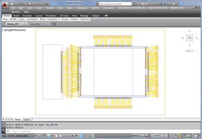
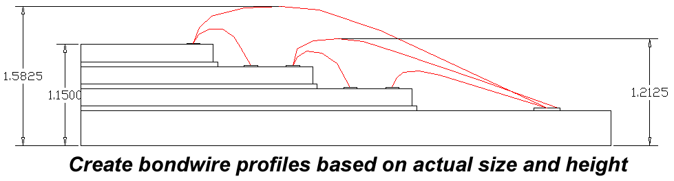
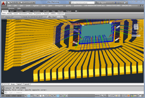
Creates 3D models of bond wires by combining a side view profile (unlimited numbers of profiles can be made) with the top view of the wires.
Key Features:
-
Automatic Setup from pre-configured stackup data set in the Hispeed command or an optional manual override with easy to use controls.
-
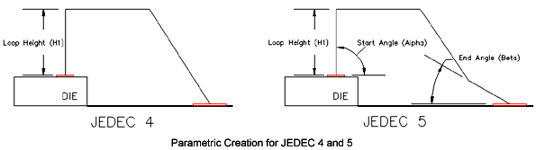
Uses custom bondwire profiles that can be differently assigned to each wire.
-
Many 3D viewing and rendering options built in.
-
ACIS compatible option so 3D files can be sent to popular modeling programs such as Solidworks and other ACIS compatible programs.
-
Stores and reads back stackup data files.
-
Makes voids where holes go through pads and vias.
-
Makes voids in cavities on either side of the substrate.
-
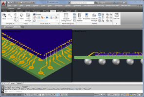
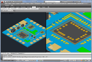
Automatically adds 3D solder balls to BGAs.
-
Allows manual control of elevation and thickness of each entity.
-
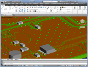
Extrudes traces, pads and components to make a 3D view of the layout.
-
Creates plating inside PCB holes.
-
Each component has an editable height that is a built in attribute.
-
Create 3D models for Lead Frame, IC Packaging, PCBs, RF and Ceramic MCM designs.
The 3D system can have a tremendous impact on the time spent in design and analysis, and thus on your company’s bottom line. In cooperation with the world’s leading companies, CAD Design Software provides award-winning layout solutions to address today’s most demanding technologies across all industries. All CAD Design Software layout systems feature 3D as a key part of the software design. Among the features are:


-
3D solid models – A true 3D solid modeling graphics engine, based on the ACIS kernel, guarantees 100% compatibility with all Mechanical CAD applications. 3D models can be generated automatically at any time, including realistic bondwire profiles. This provides the ideal PLM-style data storage solution to ensure that all members of your team can communicate and collaborate on engineering projects using a concurrent design system, not a sequential one.
By incorporating 3D in your design process, you can significantly boost your team’s efficiency, and you can reduce design rework cycles and errors. More importantly, a modern layout system can be the gateway to innovation and development of better products and additional business in your organization.
As your software technology partner, CDS is committed to making your goals a reality. What you now do in a week, you could be doing in a day. What you now do in a day, you could be doing in an hour.
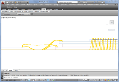
3D Bond Wires
The bondwire extrudes along the custom Bond Wire profiles to make any shape 3D bond wires. It extrudes holes and then subtracts them from the substrates, traces, pads, planes etc.
One of the most important features of any Electronic Design Automation (EDA) layout system is its 3D architecture. As designs trend toward increased speeds/densities, miniaturization of packages/modules, and integrated components with System-in-Package (SiP) technology, it is increasingly important to verify the package integrity using a modern, 3D-based system.
3D Bond Wire
Clearance Checking
2 rules for the
Advanced Design Rule Checker
software.
3D Bond Wire to Bondwire
Clearance Checker (ADRC Rule #175)

- Checks clearance between 3DPCB-created bond wires using custom profile commands.
- Will Check on multiple dies or single die with multiple wires and staggered pads bonded to elevated tiers in package (i.e. power bars, substrate)
- Will rotate in 3D space at error for viewing
3D Bond Wire Loop-Height Checker (ADRC Rule #176)

- Checks Loop Height for 3DPCB-created bond wires.
- User-Defined Datum point available (e.g. set starting point of measurement to check a height starting at a die surface, etc.)
- Error Zoom in at 45 degree angle
3D Design for Lead Frame
-
Create entire lead frame including Downsets, Gull wings and custom bondwire profiles.
3D Design for IC Packaging
-
Create Solder balls using Radius and Flatness
-
Subtract Via holes from Substrate, Pads and Traces

3D Design for PCB / RF and Ceramic MCM
-
Create through-hole vias that subtract from substrate
-
Support for creating multiple cavities and bondwire shelve assignment
-
Create and use 3D parts from library
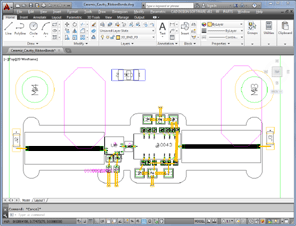
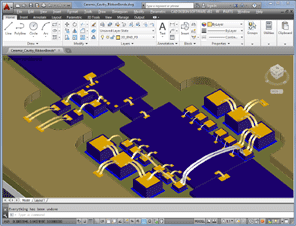
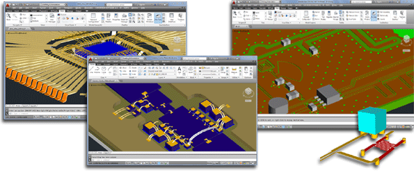
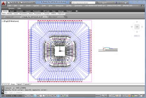
3D MCM with 3 chips, multi-level cavity:
3D RF Layout with embedded coupler:

Complex Cavity Ceramic MCM with high-frequency Ribbon Bond Wires: