Existing EPD for AutoCAD Customers Upgrade
to EPD for Windows v8.3
![]()
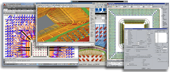
The BGA Designer Suite automates the design of all types of BGA technologies including Wire Bonded, Flip Chip, Chip Scale, Wafer Scale, Flex, and TAB Bonded.
Supports substrates: Organic, Ceramic
(LTCC) and Flex. Cavity type designs,
facing up or down, with any number of
shelves are fully supported with
optional vertical metal on the shelf
edges.
![]()
Key Features:
-
Bond-finger / bond-wire fanout uses parametric controls for unlimited creative flexibility
-
Automatic creation of JEDEC or custom BGAs including reading in an MS Excel® file with Netnames and Class names initialized
-
Automatic and interactive Netlist Creation tools for single chips and MCMs
-
Support for all package types including new technologies BGA, MCM, CSP, BUM, WSP, etc.
-
Six ways to read in die information for automatic die creation
-
Reads .LIQ files
-
Reads .DIE files
-
Reads .DWG files
-
Reads GDSII Stream files
-
Digital scans from photographs
-
Manual data entry
-
-
Automatic power rings with automatic signal name assignment from netlist or from die
-
Automatic Dogbone Array creation with option for a 2 via stair step on each Ball and many angle options
-
Automatic, any angle pre-route fanout from bondfingers to first row of BGA balls
-
Push and shove editing of adjacent traces at any angle
-
Auto trace spreading and thickening
-
Auto plating lead generator and checker
-
Automatic solder mask generator for bondfinger and balls
-
Netlist generation is automatic or interactive or customer supplied
-
Bonding fiducials parametrically generated
-
Parametric Mold Gate generation
-
Individual editing size and angle of single or multiple Dogbones made easy
-
Routing and route editing tools are refined for use on BGA packages
-
Fiducials for wirebonding and die placement are parametrically generated
BGA Layout Tools:
The IC Packaging Technology supports all types of BGA designs including Wire Bonded, Flip Chip, Flex, and TAB Bonded on any type of substrate: Organic, Ceramic (LTCC) and Flex with any technology configuration. Cavity type designs are supported with cavity up or down, with any numbers of shelves with optional vertical metal on the shelf edges.
-
Supports all BGA types:
-
PBGA, FBGA, FlexBGA, EBGA, ChipScale, Stacked Die, etc.
-
Full ACIS-based 3D modeler for visualization and 3D clearance checks.
-
-
Parts:
-
Intelligent die creation utilities based on X,Y information (ASCII),Graphics (DWG/DXF), or user parameters.
-
Automatic Bondpad Layout generator with 17+ pattern templates
-
-
Netlists:
-
Intelligent logic analysis of chip-level, package-level, and board-level
-
-
Read More about IC Packaging Technology
Die Bump / Flip Chip Tools:
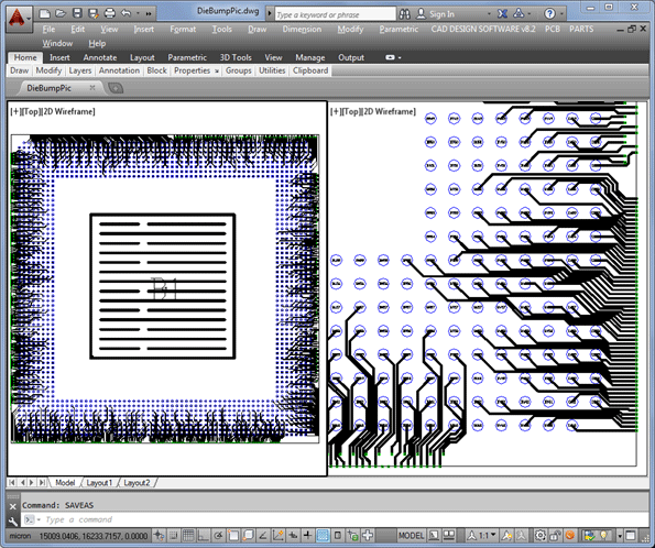
The Die Bump / Flip Chip Technology automates the process of creating redistribution routing and bump artwork to convert a standard die to a flipchip die.
-
GDSII stream file reader imports graphics from large dies and extracts relevant layers and entities by viewing a preview of the die's structure
-
BallGrid command makes patterns with a configurable number of levels and shapes for use as bumps
-
Automatic or interactive net list generation by 3 different methods
- Read More about Die Bump Technology
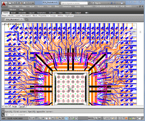
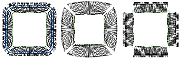
BGA Routing and Editing Tools:
The
Inter-Active Autorouter Module automates the
routing process of ball-grid array
substrates and other tight PCBs. It
contains powerful features to streamline
the routing process of dense BGA, CSP,
PCB and Hybrid / MCM designs.
-
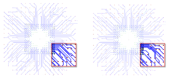
Automatic cleanup of routing to reduce unnecessary bends and segments
-
Slide vias while dragging traces with them and maintain complex, multi-level design rules
-
Powerful autorouter streamlines the routing process of dense BGA, CSP, PCB and Hybrid/MCM designs with CDS’s exclusive autorouting technology.
Angle point-to-point routing is completed quickly and automatically, shortening design cycle time.
Autofix moves, cleans and optimizes routed traces while maintaining trace-to-trace and trace-to-pad clearances.
-
Read More about Interactive Routing Utiltiy
Design Rule Checking:
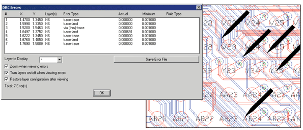
Design Rule Checker Utility is a batch clearance checking tool for user checking of completed or in-progress designs, to produce precision accuracy down to fractions of a micron.
-
Unlimited custom entity-to-entity checking.
-
Save custom DRC settings in a file.
-
View and automatically zoom to errors for correction.
-
Read more about Design Rule Checker Pro
Advanced Routing:
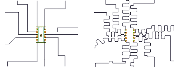
The Advanced Route Module provides many advanced tuning, filleting, chamfering, progressive chamfering, neck downs, tapering and advanced trace editing commands. The tools included enhance the features in the Master RF Suite.
-
Easy Differential Pair routing
-
Many types of length tuning.
-
Trace segment sliding.
-
Any angle advanced manual routing with on-line DRC, hugs objects and follows angles of originating pad.
-
Read More about Advanced Routing Utiltity
Dies and Wires:
-
Advanced Die Capture is possible from many sources and captures the signal names on the die.
-
Wire Diameter and length control
-
Assign bondwire profiles for single or multiple stacked die.
-
A dedicated hybrid library which allows a user to save die geometries as bare die or as part of intelligent bond wire fan outs.
-
Read More about Die and Wires
-