Existing EPD for AutoCAD Customers Upgrade
to EPD for Windows v8.3
![]()
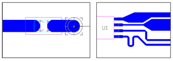
The Master Ceramic Suite is a custom-built suite that include related modules from our Technology and Utility Modules. This combination offers a complete design system for Hybrid MCM, LTCC, HTCC, Thick Film, Thin Film, both Organic and Ceramic substrates, and new, yet to be defined technologies.
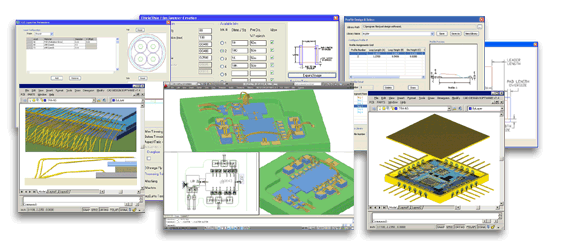
This suite of modules is built using the main EPD core product for design environment setup, stackup materials, measurement units, building component libraries, and layout tools. .
Designs can go quickly from concept to manufactured product, which will fuel more progress to bring a largely manual process to maximum automation, to include automatic masks, panels and generation of 3D analysis models. Technologies that have complex and difficult to understand design and manufacturing steps have a hard time gaining wide acceptance.
![]()
Key Features:
-
Intelligent links to wire bonding machines
-
Thick film (Rectangular, Top Hat, Right Angle) and serpentine resistor creation
-
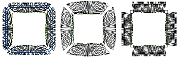
Full parameter based bondwire fanout designs with many fanout templates
-
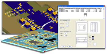
Advanced pad stack editor that edits pad shapes quickly can create custom entities on any layer at any angle or X, Y offsets. It also controls net names, class names and attribute offsets on each pin.
-
Circuits and components may be equally built up on both sides of a
thick film hybrid -
Volume / Mass report for all materials for ROHS
-
Any component (whether active or passive) can be placed on any layer,
facing up or down -
Support for Inch, Mils, MM, CM, and Microns
-
No layer, pin, entity limits
-
Advanced Die Capture is possible from many sources and captures the signal names on the die.
-
Wire Diameter and length control
-
Assign bondwire profiles for single or multiple stacked die.
-
A dedicated hybrid library which allows a user to save die geometries as bare die or as part of intelligent bond wire fan outs.
-
The die in cavity system allows for the design of cavities parametrically and graphically.
-
The parametric creation of cavities allows for:
-
Number of levels deep from either side of the substrate
-
Multiple cavity offsets from the defined base cavity for stepped cavity creation
-
Assignment of keep out perimeters for vias and traces
-
Parametrically created Dielectric masks:
|
Video Demo of DMASKS command: |

-
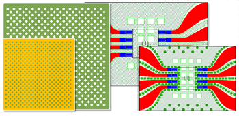
Positive Fill Planes - The industry standard method for plane creation by using a specific fill width to “paint” or “flood” the ground plane. This type of ground plane is used for creating cross-hatched or gridded planes. The ability to offset subsequent gridded planes should be available.
-
Negative Fill Planes – This type is more efficient than the positive fill method, because only the areas that will be conductor free are painted.
-
Positive Boundary Planes - An advanced plane that is modeled or enclosed by 0-width polygons, and fill pattern that displays the plane as a hatched area. This newer method allows for very fine details and accurate control over sharp corners
-
Coplanar ground shields - Create ground shields around any trace or object with other commands for creating additional via-based grounding around or on the ground shield.
-
Automatic Via Peppering - Create the optimum in additional ground plane connections, by peppering every available area of the board with vias, while maintaining DRC settings.
The Advanced Route Module provides many advanced tuning, filleting, chamfering, progressive chamfering, neck downs, tapering and advanced trace editing commands. The tools included enhance the features in the Master RF Suite.
-
Easy Differential Pair routing
-
Many types of length tuning.
-
Trace segment sliding.
-
Any angle advanced manual routing with on-line DRC, hugs objects and follows angles of originating pad
-
LTCC interconnect technology is available through a flexible via creation process, which includes support for blind/buried construction for all fired or build-up technologies. Combinations of blind/buried vias are created as blocks to form stair-stepped vias, tunnel vias (similar to through hole), straight vias, and spiral vias.
-
Via pads (catch pads) should be resizable and removable by level. Support for the addition of via fill and mixed-metal or multi-metal printings for vias should be available.
-
PCB Technology
-
Through Hole
-
Blind/Buried
-
-
MCM Technology
-
Blind/Buried
-
Stair-stepped
-
Tunnel
-
Spiral
-
-
Automatic CAM Configuration includes:
-
Gerber Output with:
-
Rotation about any point
-
Equal or Unequal X,Y Scaling
-
Mirroring on any axis, X or Y
-
Punch (drill) Output
-
Four types of Punch Optimizations
-
Panelization
-
-
Nibbler Data Auto generation and Machine Compatible Output
-
Output for wire bonding, epoxy dispense and component placement machines
-
A complete schematic and design layout tool with DRC and LVS
-
All types of Ceramic Packages supported; LTCC, HTCC, Thick Film, Thin Film
-
Advanced DRC with unlimited checking capabilities handles special LTCC rules
-
Unlimited custom entity-to-entity checking
-
View and automatically zoom to errors for correction
-
The “Ignore Errors Less Than” feature screens out insignificant minute errors not worth reviewing.
-
By grouping nets of different voltage potentials into classes, class-to-class rules may be set up for each voltage differential to enable checking of complex high-voltage power supplies.
-
Hierarchical rule setting
-
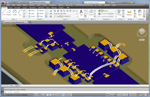
Creates 3D layers from specified set up layers
-
Creates a 3D solid for each component
-
Creates a text file for any 3D parts in a drawing
-
Allows 3D profile assignment to polylines for 3D bondwire creation
-
View PCB, substrates, all layers and components in 3D
-
3D Clearance checking of wire bonds (optional add-on)
-
GDSII:
-
Arc Vectorization Length: Controls the length of each vector.
-
Etch Compensation: Sets a negative or positive etch compensation value globally on any individual layer.
-
Automatically removes voids by splitting closed boundaries that have voids into closed boundaries with no voids.
-
Allows Scaled References: Scales a reference when a block is scaled.
-
Bi-Directional, reads in and exports to GDSII
-
Makes GDS II data from most entities
-
-
Gerber:
-
All Standard and custom fonts are converted with any style configuration including True Type Fonts
-
Recursive Paint and Scratch Capability
-
Mirrored blocks or blocks with unequal X,Y scale factors.
-
Whole families of blocks are selected for automatic flash assignment based on setting the block name prefix in a special dialog box.
-
Enter an old drawing years later and simply pick GERBOUT to make a conversion.
-
Converts DWG to Gerber in the time it takes to make a .DXF file.
-
-
Gerber In:
-
Reads any Gerber file directly
-
Can read drill and route files directly
-
Auto recognition of Gerber 274D, 274X, NC drill and NC route files.
-
Automatically reads Aperture Report files from other programs and Gerber editors.
-
Any aperture file may be read using Aperwiz.
-
Convert multiple Gerber files to separate block within one DXF file.
-
Assign unique layer names and colors to entities within the block.
-