 Chapter 01 Schematic Chapter 01 Schematic
Overview of our Schematic
program (Auto Schematic
Capture®) and how
to export the netlist for
use with placing parts,
routing and checking during
the design process.
|
Chapter 02
Technology/Setup
How to start CDS software
and setup the drawing
environment and design rules
with the Technology command. |
 Chapter 03 Chapter 03
Making Dies
Using the DIEMAKE command to
parametrically create two
die patterns and then read
in an LIQ file for the third
and then save all to a
custom library. |

Chapter 04
Attach Patterns
Using the ATTACH command to
read in the die outline
patterns and apply bondwire
fanouts. |
|
|
|
|
|
|
 Chapter 05 Chapter 05
PCB Border
Create the PCB / Boundary
outline for the design. |
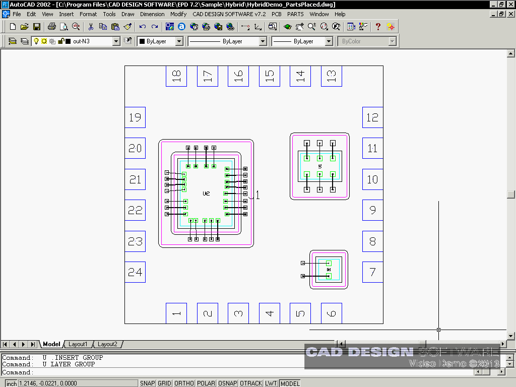
 Chapter 06 Chapter 06
Creating and Placing
components
Using the PLCC2 command to
parametrically create a PLCC
component and then using the
PLACEATTACH place and block
the attach patterns in the
drawing. |
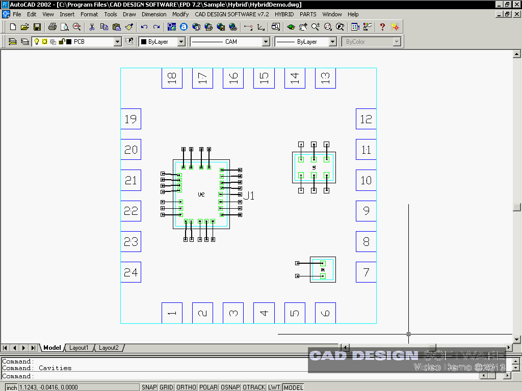 Chapter 07 Chapter 07
Creating Cavities
Using the CAVITIES command
create the cavity keep out
pattern. |
 Chapter 08 Chapter 08
Placing additional
components
Using the Parametric
Libraries to place
components in the drawing (SM Chips,
Thick Film Resistors, TOPHAT
100 Ohm Resistor,
RIGHT-ANGLE 75 Ohm
Resistor) |
|
|
|
|
|
|
 Chapter 09 Chapter 09
Creating Hybrid Vias
Using the HYBVIA command to
create and define vias in
the drawing. |
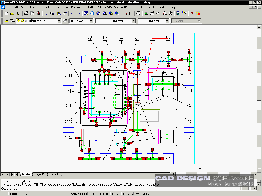
 Chapter 10 Chapter 10
Reading netlist, rat line connections
Using the NETREAD command to
read in the design netlist
and then using the RAT
command to draw the rat line
connections for routing and
placing ground ties. |
 Chapter 11 Chapter 11
Creating Ground Ties
Using the TIEVIA command to
automatically create ground
ties on the Ground nets on
multiple layers. |
 Chapter 12 Chapter 12
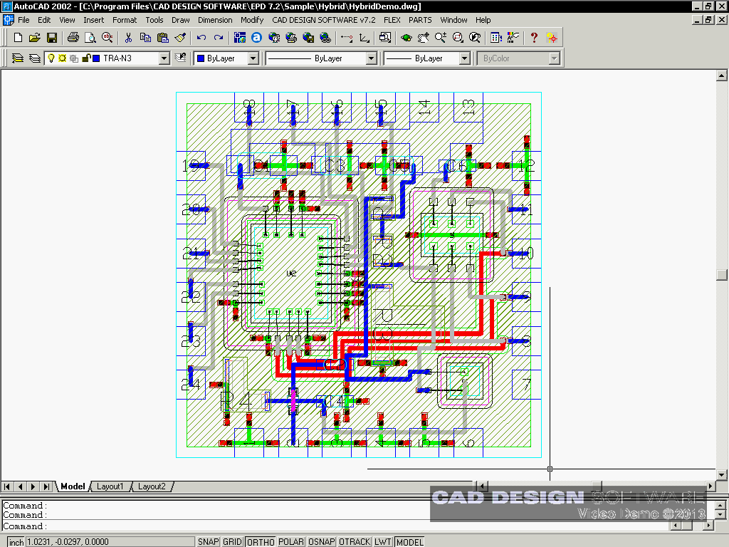
Nearside (N3)
Routing (part
1)
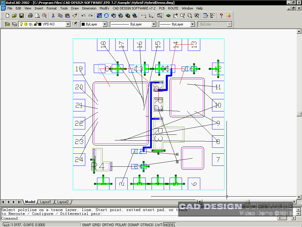
Using the TRACK command to
route on the N3 layer |
|
|
|
|
|
|
 Chapter 12 Chapter 12
Internal (N3-N2) Routing
using Vias
(part 2)
Using the TRACK command to
route on two layers and
using the via that was
defined |
 Chapter 12a Chapter 12a
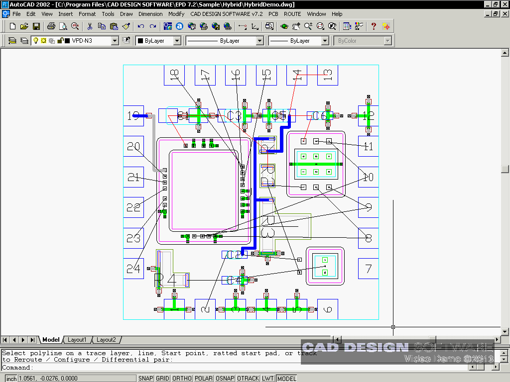
Internal (N3-N2-N1) Routing
Multiple Nets
(part 3)
Using the TRACK command to
route on multiple layers and
nets |
 Chapter 13 Chapter 13
Creating
Crossover Traces
Using the DPATCH command to
places dielectric patches
and bridges where traces on
the same layer cross. |
Chapter 14
Creating
Boundary Nets
Creating a closed 0-width
polyline that encapsulates
pins on components. This
will show how EPD can use
boundary nets that act as
conductive trace
connections. |
|
|
|
|
|
|
 Chapter 15 Chapter 15
Creating the ground plane
for F1 and N1
Using the GNDEDGE command to
create the edge boundary for
the lane and then using the
POUR command to create the
plane pattern. |
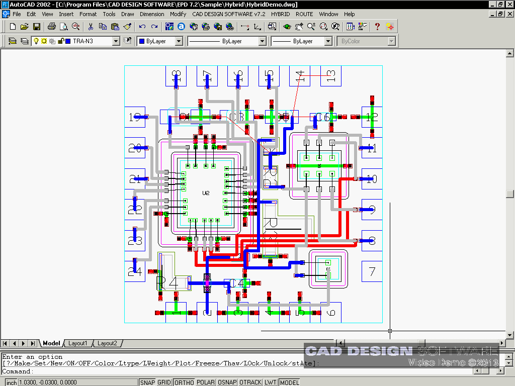
 Chapter 16 Chapter 16
Checking the net connections
Using the NETCHK command to
check for net errors then
using the Schematic netlist
as a reference netlist and
compare to the new netlist. |
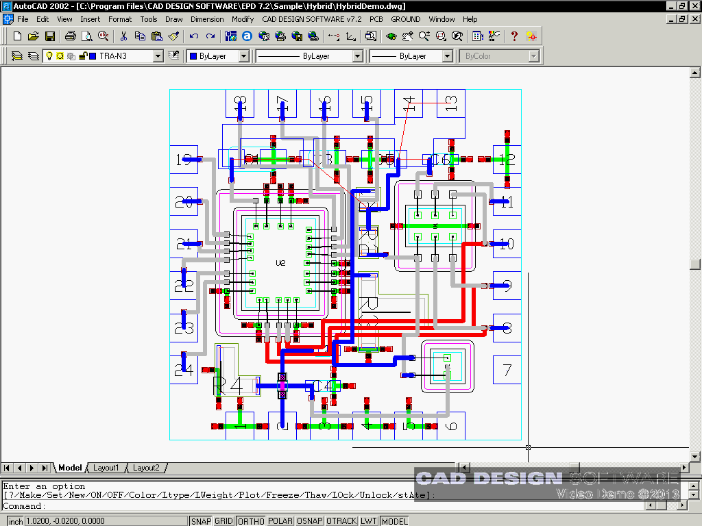
 Chapter 17 Chapter 17
Checking the design for
clearance errors
Using the DRC command to
check the board for
clearances errors and view
any errors |
Chapter 18
Creating
Dielectric offsets
Using the DVIA command to
create a "0.002” offset for
dielectric clearances on the
DEL-N1 layer |
|
|
|
|
 Chapter 19
Generating Chapter 19
Generating
Gerber files
Using the GERBOUT command to
generate the Gerber artwork
files |
 Chapter 20 Chapter 20
Viewing the
Gerber files
Using the GERBVIEW command
to view the final artwork
files |
|
|
|
|