All Technologies covered by Electronics
Packaging designer (EPD) are based on
real world design steps based on
feedback from experienced designers.
Unlike many EDA tools, the EPD design
flow and command sequence logically
follows steps that designers prefer to
use. Each of the technologies listed
below provides a powerful tool for a
specific design type.
Pick a Technology below to learn more on
how EPD Suites and Utilities help
designers create fast and accurate
designs using one of the most advanced
and complete toolsets on the market.
|
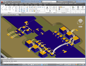
Ceramic MCM / LTCC Technology
Supports designs for all types of MCM
technologies. A dedicated hybrid library
allows
a user to save bare die and dies
with wires.

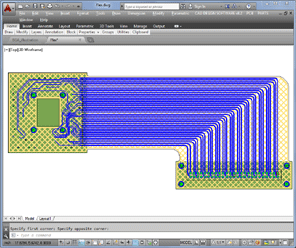
RF / Microwave Technology
Provides tools that enhances
the design of
RF / Microwave
/ Wireless printed circuit
boards
and creation of
complex embedded circuits.
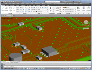
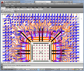
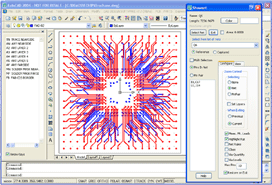
PCB Technology
The PCB layout environment
is a core set of tools
to
natively supports all major
features for PCB
circuit
design technologies.
Flex Technology
Provides tools to speed up the design of
flexible
printed circuits with true arcs teardrop
fillets with
in DRC and Gerber files.
|
Lead Frame Technology
Semi-automatic, yet extremely fast
process to
turn Lead Frame designs that
were manually
drawn to the standard CDS
data format.
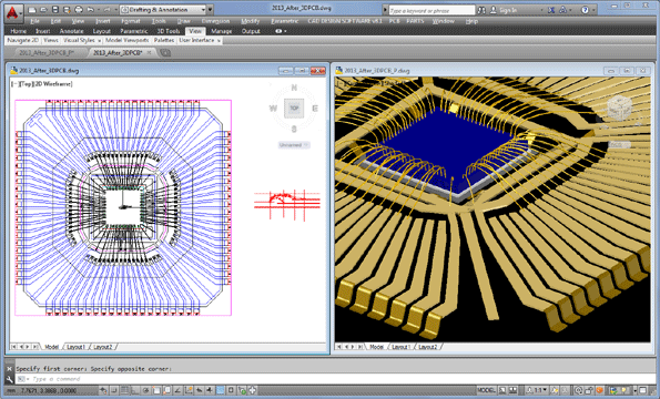
IC Packaging Technology
Contains powerful tools that have been
developed
in direct response to the
needs of the world’s
largest packaging and layout companies.
Flip Chip / Die Bump Technology
Automates the process of creating
redistribution
routing and bump artwork
to convert a standard
die to a flipchip
die.
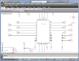
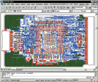
Schematic Layout Design
A full featured schematic program
capable of
quickly laying out schematic
diagrams and
outputting netlists to most
popular formats.
|