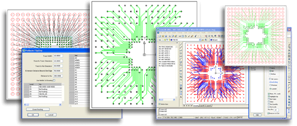
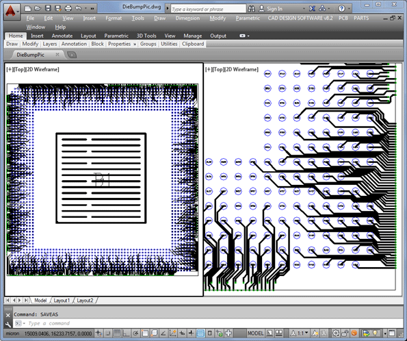
The Die Bump / Flip Chip Technology automates the process of creating redistribution routing and bump artwork to convert a standard die to a flipchip die. The redistribution layer can be created easily and quickly directly on the IC through the use of our automated bump creation and Interactive Autorouting utilities.
Key Features Include:
-
GDSII stream file reader imports graphics from large dies and extracts relevant layers and entities by viewing a preview of the die's structure
-
BallGrid command makes patterns with a configurable number of levels and shapes for use as bumps
-
Automatic or interactive net list generation by 3 different methods
-
Autorouter designed for dense BGA routing with just enough clearance
-
See the Inter-Active Autorouter Module
-
-
Complete netlist verification and DRC
-
Wafer Array command panelizes the design in perfect alignment with the original silicon image
-
Easy die creation tools can create dies from .LIQ .DIE .DWG GDS Digital scans (with distortion compensation) and manual data entry into parametric dialog box
-
Automatic orientation of die for redistribution on silicon design or for later substrate routing.
-
Routing using automatic length tuning and matching.
-
Differential pairs are interactively routed.