The Design Rule Checker Pro is a batch clearance checking tool for user checking of completed or in-progress designs, to produce precision accuracy down to fractions of a micron.
* Design Checker Lite version (DRCL) is a 2D clearance checker that shares most of its features with DRC Pro, except it is limited to standard EPD entities and non-hierarchical rules.
*CDS also offers an Advanced DRC product for more complex and custom rule checking. It also includes a library of Pre-defined packaging rules for Manufacturing and Assembly rule checking. See the Advanced DRC Module.
Each
error pointer also contains the error
information for easy viewing. Areas for
defining errors include: board edge,
component outline, bond wires,
ground-plane edge, pads, all SMT
terminal types, traces, through vias,
blind vias, holes, mounting holes,
dielectric, silk screen, and user
definable entities. You
begin by selecting the nets and layers
you want DRC Pro to check. You may
choose all of your nets, classes of
nets, or a single net or between
selected nets. Rules may be set
between classes to check with all
layers, selected layers or
layer-to-layer configuration. After
selecting nets and layers, you set
clearance rules from any object to any
other object and specify a minimum
clearance to check. Many rule sets may
be made and stored in the same layout
and run simultaneously. Errors may be
marked as acceptable and may be masked
or unmasked. A list of all rules and
errors may be printed out. Rules
may be set as “same net”, otherwise
violations between a net and itself are
ignored.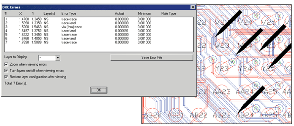
Key Features:
Unlimited custom entity-to-entity checking.
Save custom DRC settings in a file.
View and automatically zoom to errors for correction.
The Ignore Errors Less Than feature screens out insignificant minute errors not worth reviewing.
Hierarchical rule setting.
DRC rule value settings are stored in drawing database.
Rules may be set to check clearance between any two entities on the PCB.
Unlimited configuration of net-to-net and layer-to-layer checking.
By grouping nets of different voltage potentials into classes, class-to-class rules may be set up for each voltage differential to enable checking of complex high-voltage power supplies.