Existing EPD for AutoCAD Customers Upgrade
to EPD for Windows v8.3
![]()
The Value PCB Designer is a low-cost, high performance package for design of simple printed circuits. It offers the power of our high-end design suites to users that don't need the additional functions required for more complex layouts.
This suite is built using the main EPD core product for design environment setup, stackup materials, measurement units, building component libraries, and layout tools. Value PCB is suitable for all types of PCBs including Digital, Analog and most types of RF PCBs. Easy to learn and value-priced, this Suite includes a tutorial and one year maintenance contract are standard features.
![]()
Key Features:
-
Any component (whether active or passive) can be placed on any layer, facing up or down
-
Support for Inch, Mils, MM, CM, and Microns
-
No layer, pin, entity limits
-
Advanced pad stack editor that edits pad shapes quickly can create custom entities on any layer at any angle or X, Y offsets. It also controls net names, class names and attribute offsets on each pin.
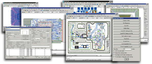
PCB Design Tools
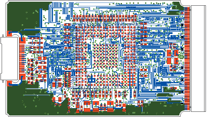
The PCB layout environment is the heart of the Master PCB Designer system. It natively supports all major features for PCB laminate circuit design technologies. The environment features an advanced Technology system, which is used to control and manipulate design rules, layering system, routing assignments, environment preferences, etc.
-
Large, parametrically controlled parts library through which an infinite number of components can be constructed
-
A dedicated suite of utilities allows construction of custom components with any imaginable geometry
-
Advanced routing tools including manual, interactive, and fully automatic modes
-
Custom entity system for customer-specific requirements
-
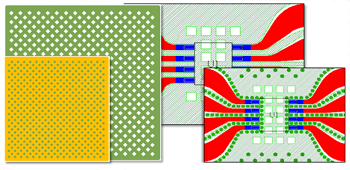
Advanced region modelers for the most advanced ground planes, including solid fill, hatched, positive, negative, and boundary fill planes
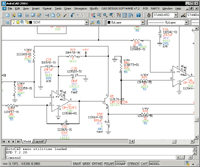
The Schematic design environment is a full featured, hierarchical schematic capture program that can communicate seamlessly with the PCB layout. The Schematic environment also features:
-
Schematic driven design rules
-
Symbols and attributes can be loaded from a database
-
Powerful library system for custom symbols
Design Rule Checking:
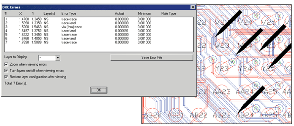
Design Rule Checker Utility is a batch clearance checking tool for user checking of completed or in-progress designs, to produce precision accuracy down to fractions of a micron.
-
Unlimited custom entity-to-entity checking.
-
Save custom DRC settings in a file.
-
View and automatically zoom to errors for correction.
-
The Ignore Errors Less Than feature screens out insignificant minute errors not worth reviewing.
-
Hierarchical rule setting.
-
DE command lists error data on selected Error Flags.
-
VE command displays all rule errors in a grid.
-
Settings stored in drawing database.
-
All errors are flagged.