Existing EPD for AutoCAD Customers Upgrade
to EPD for Windows v8.3
![]()
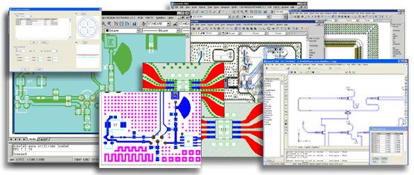
The Master RF Suite is a custom-built suite that includes RF design related modules from our Technology and Utility Modules. The system features an integrated and seamless environment in which designers can create mixed technologies for the most challenging PCB designs.
Design layouts with full intelligence on all parts, complex routing, multi-layer ground plane generation and many automated tools to dramatically reduce layout time.
Master RF Designer includes an unlimited design environment. Its geometry engine puts the power of the most advanced CAD systems at the circuit designer's fingertips. For the first time, this package brings to the EDA world an unrivaled capability to successfully and intelligently layout the most complex designs, without compromises in accuracy.
Key Features Include:
-
RF vias are made with additional vias as shields around the signal via using parametric controls
-
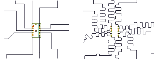
Length tuning of net lengths using arcs, accordion or trombone tuners (includes phased-array design tools)
-
Automate the creation of complex embedded circuits, Dividers, couplers, spiral inductors, radial stubs.
-
Any footprint can be made with any shape using closed polyline boundaries.
-
Via peppering makes via arrays connecting identical plane nets, on multiple layers and automatically removes vias that would connect to the wrong net
-
Path tuning for phased array antennas
-
Support for embedded components and circuits inside blocks
-
Full net list (LVS) and DRC checking functionality on any shape and at any hierarchical level
-
Creates coplanar ground shields with coplanar vias, even on arced entities automatically
-
Automatic placement of all ground ties on SMT parts, on all layers and nets with automatic tie segment / via reduction based on DRC results
-
Boundary ground planes with progressively filleted corners and variable individual gap control on every entity
-
Automatic placement of all ground ties on through hole parts, on all layers, with automatic tie spoke deletion based on DRC results
-
Split plane edges are automatically generated from simple easy to draw dividers
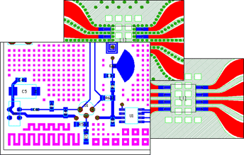
The RF Layout environment features a comprehensive library of parametrically controlled standard RF elements. It provides the electrical intelligence to all custom element and component constructions. The RF environment also features:
-
Powerful boundary based geometry, or “anyshape” nets
-
Support for true RF miters and fillets with true arcs
-
Manual and automatic features for matched lengths, differential pairs, etc.
-
Automatic length tuning and matching
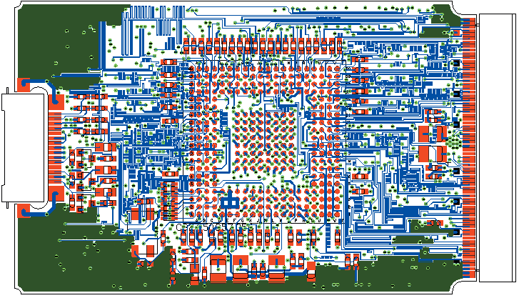
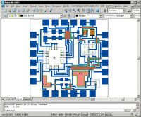
The PCB layout environment is the heart of the Master RF Designer system. It natively supports all major features for PCB laminate circuit design technologies. The environment features an advanced Technology system, which is used to control and manipulate design rules, layering system, routing assignments, environment preferences, etc.
-
Large, parametrically controlled parts library through which an infinite number of components can be constructed
-
A dedicated suite of utilities allows construction of custom components with any imaginable geometry
-
Advanced routing tools including manual, interactive, and fully automatic modes
-
Custom entity system for customer-specific requirements
-
Advanced region modelers for the most advanced ground planes, including solid fill, hatched, positive, negative, and boundary fill planes
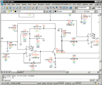
The Schematic design environment is a full featured, hierarchical schematic capture program that can communicate seamlessly with the circuit layout. The Schematic environment also features:
-
Schematic driven design rules
-
Symbols and attributes can be loaded from a database
-
Powerful library system for custom symbols
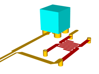
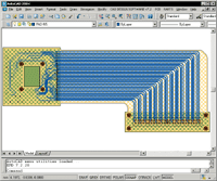
The Ceramic layout environment provides all of the tools and utilities to create die assemblies in a wirebonded configuration. All major build up construction types are supported, with custom cavity cutouts, cavity sidewall plating, and micro via/via-in-via technology. The Ceramic environment also features:
-
Automatic, parameter-driven pad layout diagrams
-
On the fly bare die assembly routing and manipulation
-
Support for Laminate, Co-fired Ceramic (including LTCC), Thick Film, and Thin Film constructions
-
Hybrid vias with Via Fill, Dielectric openings, and stair stepped configurations
-
Dielectric patch crossover options
The Flex Layout environment features include support for flex tape based designs, as well as rigid-flex combinations. It provides special step and repeat features for easy constructions of panels. The Flex environment also features:
-
Automatic and progressive teardrops
-
Custom coverlay openings
-
Timesaving utilities, such as automatic and progressive trace filleting
The Advanced Route Module provides many advanced tuning, filleting, chamfering, progressive chamfering, neck downs, tapering and advanced trace editing commands. The tools included enhance the features in the Master RF Suite.
-
Easy Differential Pair routing
-
Many types of length tuning.
-
Trace segment sliding.
-
Any angle advanced manual routing with on-line DRC, hugs objects and follows angles of originating pad
Manufacturing and
Gerber Artwork outputs:
The Master RF Designer system features
powerful
fabrication outputs, such as automatic
drill tables, drill
charts, NC drill files, and Laser
control outputs. A number
of common tasks are completely automated
by
intelligent, parameter driven programs.
The system also
features:
-
Automatic soldermask openings
-
Automatic silkscreen generation and positioning
-
Automatic assembly drawings
-
Automatic equipment outputs to wirebond, pick and place, and epoxy dispense machines (Contact CDS to find out which machines are currently supported)
-
DWG, DXF
-
Powerful Gerber output
-
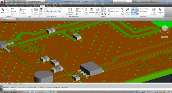
3D visualization of design created as true 3D model
-
3D modeling for accurate data output to mechanical and analysis systems
-
Subtract Vias and Holes from Substrate, Pads and Traces.
-
Create Cylindrical Holes and specify Hole Wall Thickness.
-
Industry standard outputs (ACIS, IGES, STEP)
-
True 3D solid creation, with exports to all popular MCAD systems through ACIS, IGES, STEP